Build this PWM Signal Generator Circuit
By Aditya Agarwal View In Digital Edition
Pulse-width modulation (PWM) is a technique for varying the width of electrical pulses to control the amount of power delivered to a device. It allows for precise control, as well as efficient energy consumption. PWM is particularly suited for running inertial loads such as motors in robots.
This circuit is a PWM signal generator that is constructed solely using digital logic circuits. The aim of this project is to understand a technique to produce PWM signals using fundamental digital circuits such as timers, latches, logic gates, and transistors, without any ready-to-use ICs (such as a 555 timer).
The circuit can be used practically to increase the number of PWM outputs of a microcontroller, or in an FPGA design to generate PWM signals. Besides the components in the Parts List, 18 LEDs can be used optionally to see the value in the register, timer, the Zero-Flag, and the Equal-Flag, respectively. A detailed explanation of each stage of the circuit and how it works is provided.
| Component | Qty |
| 74HC74 Dual D-Latch ICs | 4 |
| 74HC590 Up-Counter IC | 1 |
| 74HC86 Quad XOR Gate ICs | 2 |
| 74HC00 Quad NAND Gate IC | 1 |
| Diodes | 8 |
| 2N2222 Bipolar Junction Transistors | 2 |
| 220 ohm Resistors | 2 |
| 1K ohm Resistors | 2 |
| Breadboard | 1 |
| DIP Switches | 8 |
| Pushbutton | 1 |
| Pulldown Resistors | 9 |
| Wires | - |
Parts List.
In brief, the circuit consists of an eight-bit timer which counts as a clock input as is provided to it. When the timer overflows to zero, the output is switched on, which indicates the start of a pulse. When the timer reaches a value stored in a register, the output is switched off, which indicates the end of a pulse. Using this technique, the width of each pulse can be precisely controlled by changing the value in a register. This design also allows the resolution of the circuit to easily be scaled.
The Circuit and How It Works
This section explains the design of the circuit and the steps it follows to generate one complete pulse. The logic diagram of the circuit is shown in Figure 1.
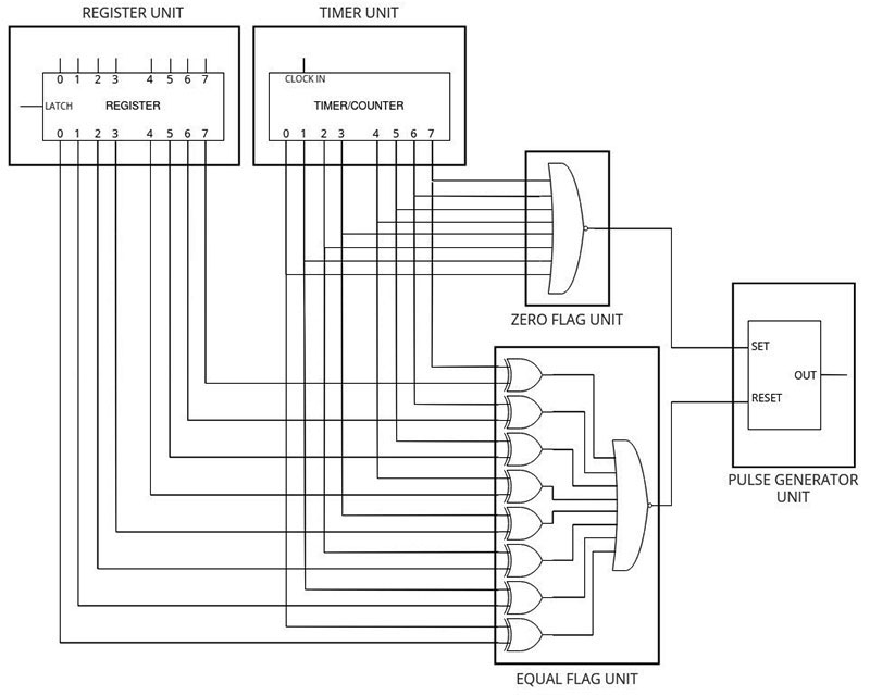
Figure 1 - Logic diagram of the PWM signal generator circuit.
The purpose of each component is listed in Table 1.
| Component | Purpose | Input | Output |
| Register Unit | Stores the required duty cycle of the PWM signal. | Eight-bit value (from user) — latch signal. | Stored eight-bit value (given by user). |
| Counter/Timer Unit | Provides a counter for measuring pulse width. | Clock oscillator. | Eight-bit value (counts from 0-255). |
| Zero-Flag Unit | Checks when the value of the counter is 0, i.e., the beginning of a pulse. | Eight-bit value from timer. | One-bit value (true when the counter value is 0, otherwise false). |
| Equal-Flag Unit | Checks when the value of the timer matches that of the register, i.e., the end of a pulse. | Eight-bit value from timer and eight-bit value from register. | One-bit value (true when the counter value matches the register value, otherwise false). |
| Pulse Generator Unit | Latches to a high (or low) state based on the outputs of the Zero-Flag and Equal-Flag. | Zero-Flag (to set input) and Equal-Flag (to reset input). | PWM wave. |
Table 1.
Initially, the timer will have a value of 0. A clock input is fed into it, allowing it to start counting up to 255. Meanwhile, the desired duty cycle of the PWM signal (between 0 and 255) is stored in the register.
Whenever the timer overflows back to 0, the Zero-Flag gets activated and outputs a pulse to the Set-Input of an SR-Latch. This causes the latch to go into the Set State, i.e., its output is turned on. This is the start of a pulse.
Similarly, when the timer’s value reaches that of the register, the Equal-Flag gets activated and outputs a pulse to the Reset-Input of the SR-Latch. This causes the latch to go into the Reset State, i.e., its output is turned off. This is the end of a pulse. By using this technique, the width of a pulse can be controlled by modifying the value in the register. Those who are familiar with Arduinos may notice how similar this is to the analogWrite function, which also accepts a value between 0 and 255, and uses this to set the duty cycle of a PWM signal on a pin.
As an example, let’s require a PWM signal with a duty cycle of 10%; 10% of 256 is ~26 (00011010 in binary), which we store in the register. Initially, the timer starts at 0, which is when the Zero-Flag sets the SR-Latch, starting a pulse. As the timer counts towards 26, the output of the SR-Latch stays high, i.e., the pulse is continued. On reaching 26, the Equal-Flag resets the SR-Latch, thus ending the pulse. As the counter counts towards 255, the output of the SR-Latch stays low, so no new pulse is started. This process is repeated once the counter overflows back to 0. The pulse remains on for 26 counts and off for 230.
Note that (on paper) a race condition arises when the value in the register is set to 0, as the Zero-Flag and Equal-Flag try to simultaneously change the state of the SR-Latch. Practically, this doesn’t occur because the Equal-Flag circuitry (explained in the later sections) takes slightly longer to generate its pulse. This allows the Reset-Input of the SR-Latch to be set immediately after its Set-Input while still maintaining a duty cycle of practically 0. In the following sections, we’ll go over the construction of the individual components of the circuit.
Construction of the Register Unit
The Register unit is used to store the desired PWM duty cycle. This example uses four 74HC74 ICs. Each IC has two D-Latches, and four can be used to construct an eight-bit wide register (Figure 2).
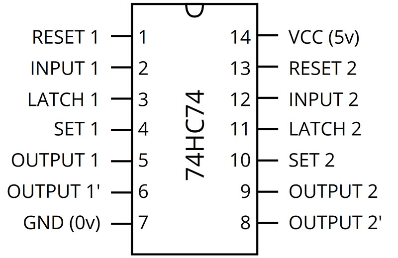
Figure 2 - Labeled diagram of the 74HC74 D-Latch IC.
The Register unit schematic is shown in Figure 3.
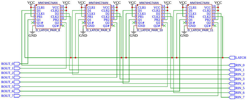
Figure 3 - Schematic of the Register unit.
The register stores values whenever its Latch-Input transitions from a low state to a high state. The value of its input pins during this short period is remembered by the register, meaning it can be read on its output pins. To store a number, set the input pins to the bits from the binary representation of the number. When a bit is 1, its corresponding pin must be connected to 5V, otherwise 0V.
Construction of the Timer Unit
The Timer unit is used to provide a counter for measuring the width of pulses that is used while calculating the start and end of each pulse. This example uses a 74HC590 Up-Counter IC (Figure 4).
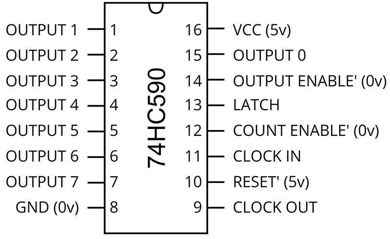
Figure 4 - Labeled diagram of the timer 74HC590 Up-Counter IC.
Each IC has one eight-bit counter. The schematic of the Timer unit is shown in Figure 5.
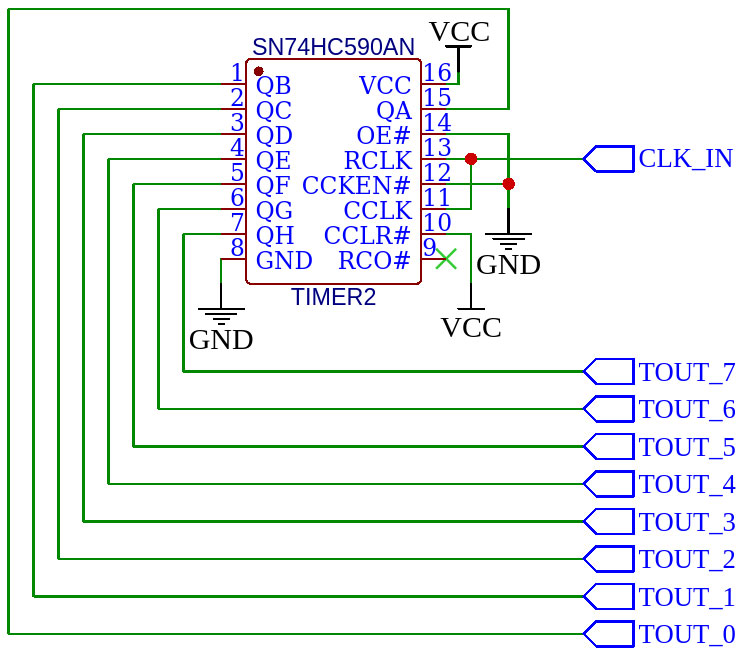
Figure 5 - Schematic of the Timer unit.
The timer counts up whenever its Clock-Input transitions from a low state to a high state.
Construction of the Zero-Flag Unit
The Zero-Flag is used to check whether the value of the counter is 0, which indicates the start of a pulse. When all the outputs of the counter are low, the Zero-Flag must output a single high bit (low otherwise). This can be constructed using an eight-input NOR gate.
The truth table of the NOR gate states that its output is true/high only when all its inputs are false/low. This example uses eight diodes and a 2N2222 NPN BJT (bipolar junction transistor) to construct the eight-input NOR gate. The diodes together act as an OR gate whose output is inverted using the BJT. The schematic of the Zero-Flag unit is shown in Figure 6.
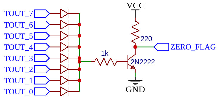
Figure 6 - Schematic of the Zero-Flag unit.
Construction of the Equal-Flag Unit
The Equal-Flag is used to check whether the value of the counter and register match, which indicates the end of a pulse. When all the corresponding pairs of bits between the timer and register match, the Equal-Flag must produce a single high bit (low otherwise). This can be constructed using eight two-input XOR gates and one eight-input NOR gate.
The truth table of the XOR gate shows that its output is true/high only when its inputs have different truth values. This process is repeated for all eight pairs of corresponding bits between the register and timer. The outputs are aggregated using an eight-input NOR gate, whose output will only be true/high when all the XOR gate outputs are false/low (i.e., all the pairs of bits match).
In this example, we have used two 74HC86 ICs (Figure 7).
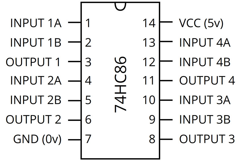
Figure 7 - Labeled diagram of the 74HC86 XOR gate IC.
Each IC has four XOR gates, and two can be used to match two eight-bit values. The NOR gate is constructed in the same way as the Zero-Flag. Figure 8 shows the schematic of the Equal-Flag unit.
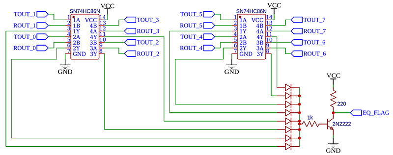
Figure 8 - Schematic of the Equal-Flag unit.
Construction of the Pulse Generator Unit
The SR-Latch is used to generate the resultant PWM signal based on the Zero-Flag and Equal-Flag. This can be constructed using four NAND gates. In this example, a single 74HC00 IC has been used (Figure 9).
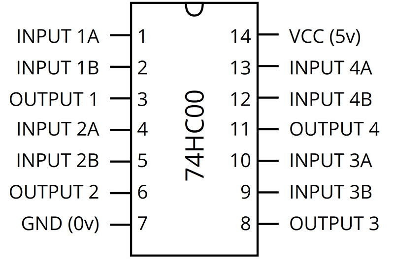
Figure 9 - Labeled diagram of the 74HC00 NAND gate IC.
Each IC has four NAND gates, which can be used to construct the SR-Latch. The schematic of the SR-Latch constructed using four NAND gates is shown in Figure 10.
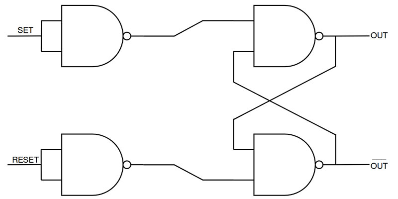
Figure 10 - Schematic of the SR-Latch constructed using four NAND gates.
Figure 11 is the schematic of the Pulse Generator unit.
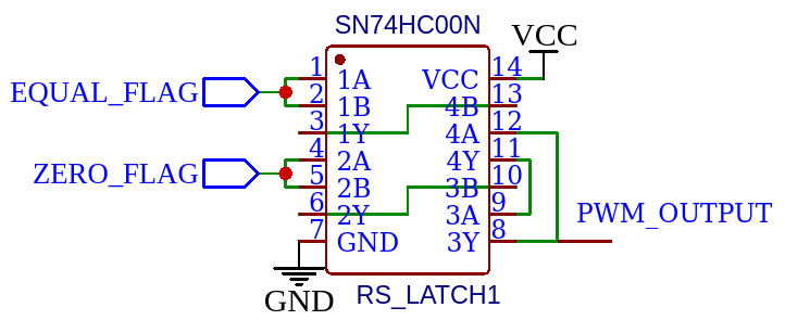
Figure 11 - Schematic of the Pulse Generator unit.
The Complete Circuit
The schematic of the complete circuit is in Figure 12.
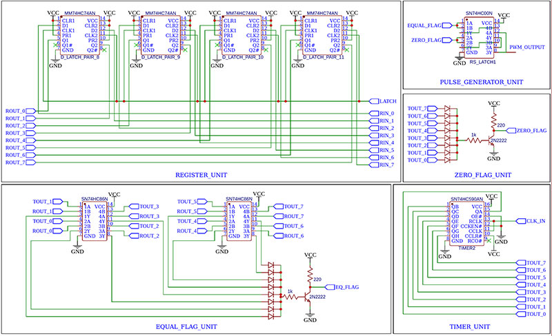
Figure 12 - Schematic of the complete circuit.
The circuit constructed on a breadboard is shown in Figure 13.
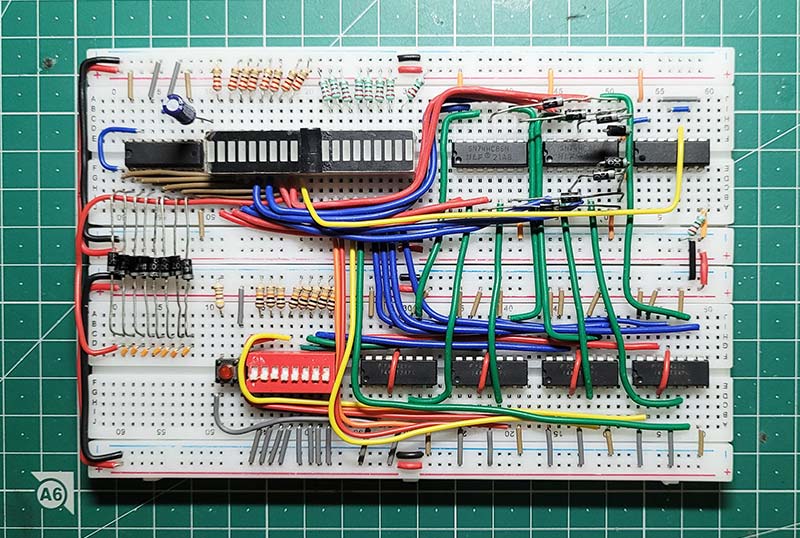
Figure 13 - Circuit constructed on breadboard.
The breadboard has a few extra components (switches, LED array, and pushbutton) that are not included in the schematic. These are used for testing the circuit. A capacitor has been used to provide AC coupling for the clock input to the timer. A top view of the PCB (printed circuit board) layout of the circuit is shown in Figure 14.
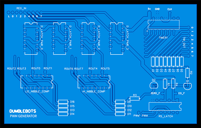
Figure 14 - PCB layout of the circuit (top view).
The layout of the bottom is shown in Figure 15.
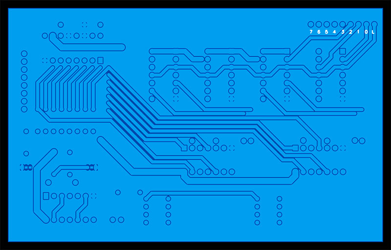
Figure 15 - PCB layout of the circuit (bottom view).
In this example, the resolution of the circuit is only eight bits (256 discrete levels can be selected for the output). The design allows the resolution to be arbitrarily increased by daisy chaining more counters and increasing the width of the register, Zero-Flag, and Equal-Flag. Note that an increased resolution will also require an increased clock frequency for the timer, as the circuit would overall take longer to count from 0.
Testing the Circuit
The circuit requires a stable 5V supply to run properly. Start by connecting a stable square wave to the clock input. You can use an Arduino, 555 timer, or function generator for this purpose.
Next, store an arbitrary value in the register using the previously mentioned method. By connecting an LED to the PWM output, it can be seen that storing lower values in the register causes the LED to be dimmer, while storing higher values causes the LED to be brighter.
Figures 16-22 are the waveforms on the various pins as shown on an oscilloscope.
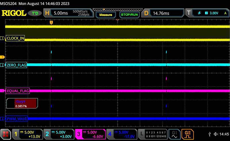
Figure 16 - Oscilloscope visualization for 0% duty cycle (value is 0).
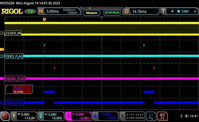
Figure 17 - Oscilloscope visualization for 10% duty cycle (value is 26).
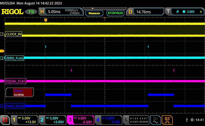
Figure 18 - Oscilloscope visualization for 25% duty cycle (value is 64)
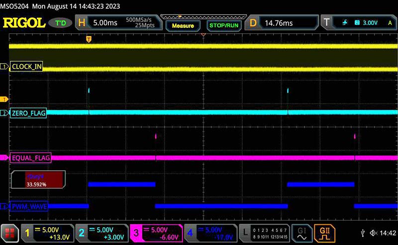
Figure 19 - Oscilloscope visualization for 33% duty cycle (value is 86).
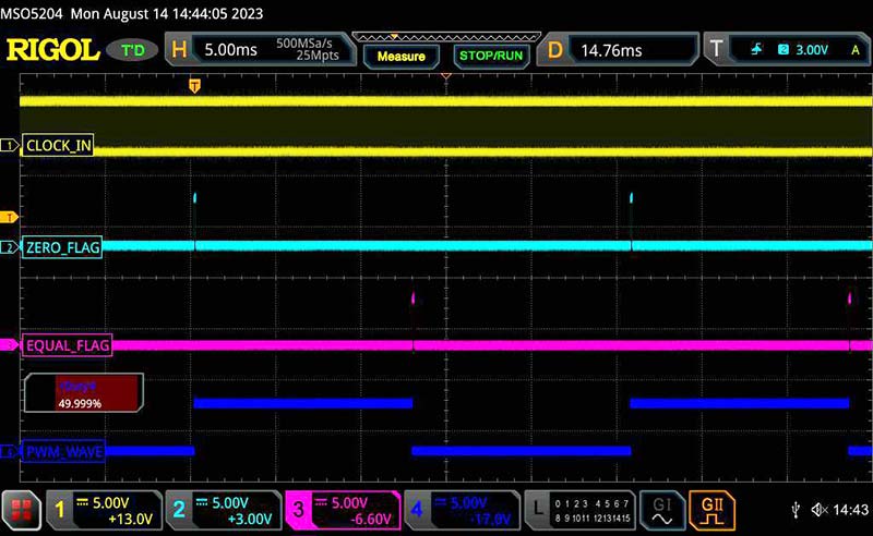
Figure 20 - Oscilloscope visualization for 50% duty cycle (value is 128).

Figure 21 - Oscilloscope visualization for 75% duty cycle (value is 192).
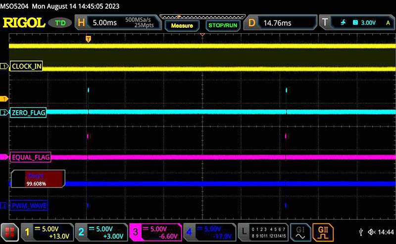
Figure 22 - Oscilloscope visualization for 100% duty cycle (value is 255).
To drive loads larger than small LEDs, an op-amp or BJT amplifier needs to be used, without which the SR-Latch might get permanently damaged.
Get Your Motors Running
The circuit can be used along with a microcontroller to increase its PWM outputs. To reduce the number of pins required, a shift-register can be used. SV
Aditya Agarwal is a dedicated university student deeply passionate about electronics, programming, and technology. He has honed these skills since a young age, delving into diverse areas such as Arduino robotics, digital circuits, systems programming, and competitive programming. With an active blog dedicated to electronics and DIY, Aditya Agarwal is eager to share his insights with readers. You can connect with him at https://linkedin.com/in/aditya-a-garwal. You can find his blog at https://dumblebots.com.
Article Comments